 EN
EN

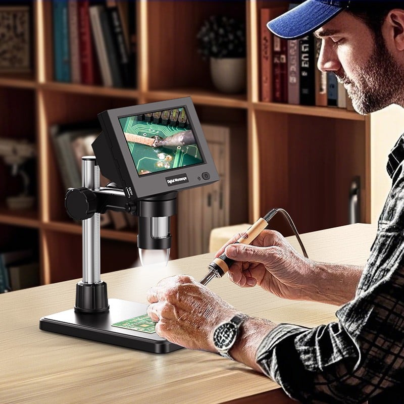
Selecting the right circuit board microscope is a critical decision that directly impacts the quality and efficiency of your electronic repair and inspection work. A properly chosen circuit board microscope enables precise component identification, accurate soldering verification, and detailed fault diagnosis across complex PCB layouts. The selection process involves evaluating multiple technical specifications, understanding your specific application requirements, and balancing performance capabilities with budget constraints.
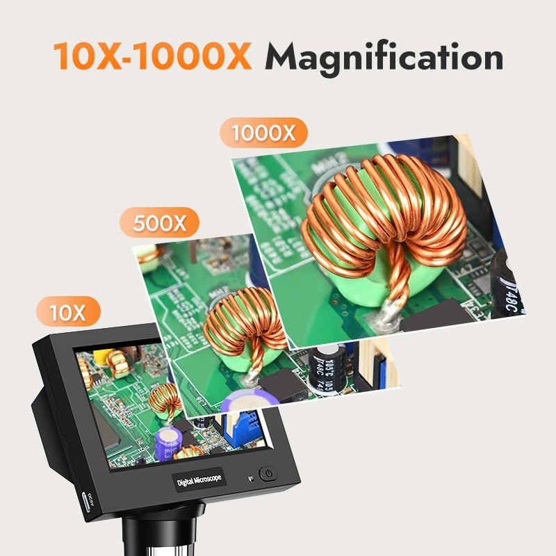
This comprehensive guide provides the essential framework for making an informed circuit board microscope selection decision. Whether you're establishing a new electronics lab, upgrading existing inspection capabilities, or expanding repair operations, understanding the key selection criteria ensures your investment delivers optimal performance. The following sections examine the critical factors that determine microscope suitability for circuit board applications, from magnification requirements to advanced imaging features.
Understanding Circuit Board Microscope Types and Technologies
Optical Microscope Configurations
Traditional optical circuit board microscopes utilize compound lens systems to achieve magnification levels suitable for PCB inspection tasks. These systems typically offer magnification ranges from 10x to 100x, providing adequate detail for component identification and basic soldering inspection. Optical microscopes excel in applications requiring true color representation and natural depth perception, making them ideal for visual component verification and general circuit analysis.
The optical design determines working distance, field of view, and resolution characteristics that directly impact usability during circuit board work. Longer working distances accommodate soldering iron access and component manipulation, while wider fields of view enable efficient board scanning. Resolution capabilities determine the smallest feature sizes that can be clearly distinguished, affecting the microscope's suitability for modern high-density circuit board designs.
Digital Microscope Technology
Digital circuit board microscopes integrate electronic imaging sensors with optical systems to capture and display magnified images on external monitors or screens. This technology offers significant advantages for documentation, measurement, and collaborative inspection tasks. Digital systems typically provide higher magnification ranges, often extending from 50x to 1200x or beyond, enabling detailed analysis of microscopic circuit features and component structures.
The digital approach eliminates eye strain associated with prolonged microscope use while enabling image capture, measurement tools, and real-time sharing capabilities. Modern digital circuit board microscopes incorporate high-resolution sensors, advanced image processing, and intuitive software interfaces that enhance productivity and accuracy. The ability to save, annotate, and compare images proves invaluable for quality control documentation and troubleshooting procedures.
Stereo Microscope Applications
Stereo microscopes provide three-dimensional viewing capabilities that enhance depth perception and spatial understanding during circuit board inspection. This technology proves particularly valuable for component placement verification, soldering quality assessment, and mechanical assembly evaluation. The dual optical paths create stereoscopic vision that helps operators judge component heights, identify bridging issues, and navigate complex board topographies.
Contemporary stereo circuit board microscopes often combine traditional optical viewing with digital imaging capabilities, offering flexibility in inspection approaches. The three-dimensional perspective facilitates precise manipulation during rework operations while reducing the risk of component damage or placement errors. Professional repair facilities frequently rely on stereo microscopes for their superior ergonomics and intuitive operation characteristics.
Essential Magnification and Resolution Requirements
Magnification Range Selection
Determining appropriate magnification requirements begins with analyzing the smallest circuit features that require inspection. Modern surface-mount components, including 0201 packages and fine-pitch connectors, demand magnification levels of 50x to 200x for adequate detail resolution. Advanced circuit board microscopes offering variable magnification provide the flexibility to examine both overall board layouts at lower magnifications and specific component details at higher settings.
The relationship between magnification level and working distance significantly impacts practical usability during circuit board work. Higher magnifications typically reduce working distance, potentially limiting tool access and component manipulation capabilities. Professional-grade circuit board microscopes optimize this balance through advanced optical designs that maintain usable working distances across extended magnification ranges.
Consider future application requirements when selecting magnification capabilities, as evolving circuit technologies continue to reduce component sizes and increase density. A circuit board microscope with expandable magnification options provides long-term value and adaptability to changing inspection demands. The investment in higher-capability systems often proves cost-effective compared to frequent equipment upgrades.
Resolution and Clarity Standards
Resolution capabilities determine the smallest distinguishable features within magnified circuit board images, directly affecting inspection accuracy and reliability. High-quality circuit board microscopes achieve resolution levels sufficient to clearly identify solder joint quality, trace continuity, and component orientation details. The combination of optical resolution and digital sensor specifications establishes overall system performance for critical inspection tasks.
Image clarity depends on multiple factors including lens quality, lighting systems, and vibration isolation characteristics. Premium circuit board microscopes incorporate precision-ground lenses and advanced coatings that minimize optical distortions and maximize light transmission. The resulting image quality enables confident identification of defects, accurate measurements, and reliable quality assessments across diverse circuit board types.
Field of View Considerations
Field of view specifications define the observable area at specific magnification levels, influencing inspection efficiency and workflow productivity. Wider fields of view enable rapid board scanning and general assessment tasks, while narrower fields provide detailed examination of specific components or features. Modern circuit board microscopes optimize field of view characteristics to balance overview capabilities with detail resolution requirements.
The practical field of view also depends on display characteristics when using digital microscope systems. Large, high-resolution monitors enhance the effective viewing area and reduce the need for frequent repositioning during inspection tasks. Professional applications benefit from microscopes that maintain usable field of view dimensions across the entire magnification range, supporting efficient workflow transitions between different inspection levels.
Lighting Systems and Illumination Quality
LED Illumination Technology
Advanced LED lighting systems provide the consistent, high-quality illumination essential for accurate circuit board inspection. Modern circuit board microscopes utilize multiple LED arrays positioned to eliminate shadows and provide uniform light distribution across the viewing field. The color temperature and intensity characteristics of LED systems significantly impact component identification, solder joint evaluation, and defect detection capabilities.
Professional LED illumination systems incorporate adjustable intensity controls and color temperature options that accommodate different circuit board materials and component types. The ability to modify lighting conditions enhances contrast and reveals surface details that might remain hidden under standard illumination. Energy-efficient LED technology also provides long operational life and stable light output compared to traditional illumination sources.
Ring Light and Incident Illumination
Ring light configurations surround the optical axis to provide shadow-free illumination ideal for circuit board surface inspection. This lighting arrangement eliminates directional shadows that can obscure component details or create false defect indications during quality assessment procedures. Modern ring light systems for circuit board microscopes offer variable intensity zones and diffusion options that optimize lighting distribution for specific inspection requirements.
Incident illumination systems direct light onto circuit board surfaces from controlled angles, enhancing surface texture visibility and three-dimensional feature definition. The combination of ring light and incident illumination provides comprehensive lighting coverage that reveals both surface details and dimensional characteristics. Professional circuit board microscopes often incorporate multiple illumination modes that can be selected or combined based on specific inspection needs.
Polarized and Oblique Lighting Options
Specialized lighting techniques including polarized and oblique illumination reveal circuit board features that remain invisible under standard lighting conditions. Polarized light reduces glare from reflective surfaces and enhances contrast for component markings and surface textures. This capability proves particularly valuable when inspecting circuit boards with conformal coatings or examining components with highly reflective surfaces.
Oblique lighting creates directional shadows that emphasize surface topology and reveal dimensional features on circuit board assemblies. This technique enhances solder joint profile visibility, component placement accuracy assessment, and foreign object detection capabilities. Advanced circuit board microscopes provide user-selectable lighting modes that enable rapid switching between illumination techniques based on specific inspection requirements.
Mechanical Design and Ergonomic Features
Stand Stability and Vibration Control
The mechanical stability of a circuit board microscope directly affects image quality and measurement accuracy, particularly at higher magnifications where small vibrations become significantly amplified. Professional-grade microscope stands incorporate heavy-duty construction and vibration-dampening materials that maintain steady imaging even in active work environments. The base design and center of gravity distribution determine overall system stability during operation.
Advanced vibration isolation systems protect sensitive optical components from external disturbances while maintaining precise focus alignment. These systems prove essential in manufacturing environments where nearby equipment operation or building vibrations could compromise inspection accuracy. Premium circuit board microscopes often feature adjustable isolation characteristics that can be optimized for specific installation conditions.
Working Distance and Accessibility
Adequate working distance between the microscope objective and circuit board surface enables tool access for rework operations and component manipulation. Professional circuit board microscopes maintain usable working distances of 50mm or greater even at high magnifications, accommodating soldering iron access and precision placement tools. The optical design optimization balances working distance requirements with magnification capabilities and image quality standards.
Stage accessibility and clearance considerations affect the maximum circuit board sizes that can be accommodated and the ease of board positioning during inspection. Adjustable stage heights and tilt mechanisms enhance accessibility for boards with varying component profiles or connector orientations. The mechanical design should facilitate rapid board loading and positioning without compromising optical alignment or measurement accuracy.
Focus Mechanisms and Precision Controls
High-precision focus mechanisms enable accurate depth positioning and maintain sharp imaging across varying component heights on circuit board assemblies. Professional circuit board microscopes incorporate fine and coarse focus controls with minimal backlash and smooth operation characteristics. The focus mechanism design determines the microscope's ability to maintain sharp focus during board manipulation and repositioning operations.
Motorized focus systems provide remote control capabilities and enable automated focus stacking for extended depth of field imaging. These advanced features prove valuable when documenting circuit board assemblies with significant height variations or when generating measurement data requiring precise focus positioning. The integration of digital focus indicators and position memory functions enhances workflow efficiency and repeatability.
Software Integration and Digital Capabilities
Image Capture and Documentation
Professional circuit board microscope systems integrate comprehensive software packages that enable high-resolution image capture, annotation, and documentation capabilities. The software interface should provide intuitive controls for camera settings, lighting adjustments, and measurement tools while maintaining responsive performance during operation. Advanced image capture features include automatic exposure optimization, white balance correction, and noise reduction processing.
Documentation capabilities extend beyond basic image capture to include measurement tools, comparison features, and report generation functions. Professional applications require the ability to create standardized inspection reports with embedded images, measurements, and analysis results. The software should support multiple image formats and provide compatibility with common documentation and quality management systems used in electronics manufacturing environments.
Measurement and Analysis Tools
Integrated measurement capabilities transform circuit board microscopes into precision metrology instruments suitable for quality control and dimensional verification tasks. Software-based measurement tools provide accurate distance, area, and angular measurements with automatic scaling based on magnification settings. Advanced analysis functions include statistical measurement reporting, tolerance verification, and trend analysis capabilities.
Professional measurement software incorporates calibration procedures that ensure accuracy across different magnification levels and optical configurations. The measurement tools should provide sub-pixel accuracy and account for optical distortions that could affect measurement precision. Integration with CAD systems and component databases enhances measurement efficiency and enables automated comparison with design specifications.
Connectivity and Network Integration
Modern circuit board microscopes provide comprehensive connectivity options including USB, Ethernet, and wireless interfaces that enable integration with existing quality management and documentation systems. Network connectivity facilitates remote access, collaborative inspection, and centralized data storage capabilities. The system should support standard network protocols and provide security features appropriate for industrial environments.
Cloud integration capabilities enable automatic backup of inspection data and provide access to inspection results from multiple locations. Professional applications benefit from systems that integrate with enterprise resource planning software and quality management databases. The connectivity features should maintain data integrity and provide audit trails suitable for quality certification requirements and regulatory compliance needs.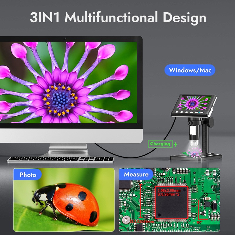
FAQ
What magnification level is needed for SMD component inspection on circuit boards?
Surface-mount device inspection typically requires magnification levels between 50x and 200x depending on component size and inspection detail requirements. Modern 0201 and 01005 components need higher magnifications around 100x to 200x for adequate detail resolution, while larger components like 1206 or SOIC packages can be inspected effectively at 50x to 100x magnification. The circuit board microscope should provide variable magnification to accommodate different component types on the same board.
How important is working distance when choosing a circuit board microscope?
Working distance is crucial for practical circuit board work as it determines tool access for rework operations and component manipulation. Professional applications require working distances of at least 50mm to accommodate soldering irons, tweezers, and placement tools. Insufficient working distance severely limits the microscope's utility for hands-on repair work and can make inspection tasks unnecessarily difficult.
What lighting features are essential for circuit board inspection quality?
Essential lighting features include adjustable LED ring lights for shadow-free illumination, variable intensity controls for different component types, and oblique lighting options for enhanced surface detail. The lighting system should provide uniform distribution across the field of view and offer different color temperature options to optimize contrast for various circuit board materials and component markings.
Should I choose an optical or digital circuit board microscope system?
Digital circuit board microscopes offer significant advantages including image capture, measurement tools, reduced eye strain, and documentation capabilities that optical-only systems cannot provide. While optical microscopes may offer superior color accuracy and depth perception, digital systems provide better overall value for professional applications requiring documentation, measurement, and collaborative inspection capabilities. Many modern systems combine both optical viewing and digital imaging for maximum flexibility.
Table of Contents
- Understanding Circuit Board Microscope Types and Technologies
- Essential Magnification and Resolution Requirements
- Lighting Systems and Illumination Quality
- Mechanical Design and Ergonomic Features
- Software Integration and Digital Capabilities
-
FAQ
- What magnification level is needed for SMD component inspection on circuit boards?
- How important is working distance when choosing a circuit board microscope?
- What lighting features are essential for circuit board inspection quality?
- Should I choose an optical or digital circuit board microscope system?