
When precision meets electronics repair and assembly work, having the right visual aid becomes crucial for success. A microscope for soldering transforms complex circuit board work from a challenging task into a manageable process, allowing technicians and hobbyists to see fine details with exceptional clarity. Modern digital microscopes have revolutionized the way professionals approach intricate soldering tasks, providing magnified views that reveal component details invisible to the naked eye. These specialized tools have become indispensable in electronics manufacturing, repair shops, and engineering laboratories worldwide.

Understanding Digital Microscope Technology for Electronics Work
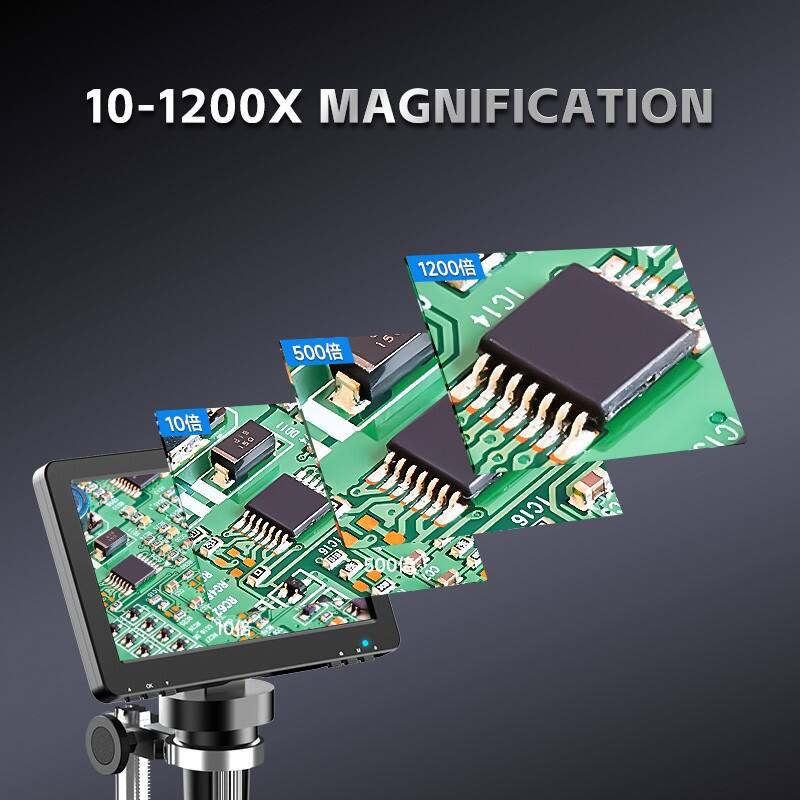
Core Imaging Components and Magnification Systems
Digital microscopes designed for soldering applications incorporate advanced CMOS sensors and high-quality optical lenses to deliver crystal-clear imagery. These systems typically offer magnification ranges from 10x to 300x, providing flexibility for various component sizes and detail levels. The integrated LED lighting systems ensure consistent illumination across the work surface, eliminating shadows that could obscure critical solder joint details. Professional-grade models feature adjustable focal distances and depth-of-field controls that accommodate different circuit board thicknesses and component heights.
The digital display technology has evolved significantly, with many modern units featuring large LCD screens that reduce eye strain during extended work sessions. Real-time image processing capabilities allow for enhanced contrast and brightness adjustments, making it easier to distinguish between different materials and surface textures on circuit boards. Advanced models also include image capture and video recording functions, enabling documentation of repair processes and quality control procedures.
Optical Performance and Resolution Specifications
Resolution quality directly impacts the effectiveness of any microscope for soldering applications, with most professional units offering at least 1080p HD imaging capabilities. Higher-end models provide 4K resolution, delivering unprecedented detail visibility for the most demanding precision work. The optical zoom functionality works in conjunction with digital enhancement to provide smooth magnification transitions without image degradation. Color accuracy becomes particularly important when identifying component markings, wire colors, and oxidation patterns on solder joints.
Frame rate performance ensures smooth real-time viewing during active soldering operations, with most quality units maintaining 30-60 frames per second at full resolution. This fluid motion tracking prevents the disorientation that can occur with lower-quality imaging systems. The combination of optical clarity and digital processing creates an enhanced viewing experience that surpasses traditional optical microscopes in many practical applications.
Essential Features for Professional Soldering Applications
Illumination Systems and Light Control
Proper lighting represents one of the most critical aspects of effective soldering microscopy, as inadequate illumination can mask defects and create safety hazards. Ring-light LED configurations provide even distribution around the viewing area, minimizing harsh shadows that could hide solder joint problems. Adjustable brightness controls allow users to optimize lighting conditions for different materials and surface finishes, from matte PCB substrates to highly reflective metallic components.
Advanced lighting systems incorporate multiple LED zones with independent control, enabling selective illumination that highlights specific areas of interest. Some models feature polarized lighting options that reduce glare from shiny surfaces while enhancing texture visibility on solder joints. The color temperature of the LED array affects how accurately users can perceive true colors, with daylight-balanced LEDs providing the most natural color reproduction for component identification.
Working Distance and Ergonomic Considerations
The working distance between the microscope lens and the circuit board determines how much space remains available for soldering tools and hand movements. Professional models typically maintain working distances of 4-8 inches, providing adequate clearance for soldering irons, tweezers, and other precision instruments. This standoff distance also prevents accidental contact between hot soldering equipment and the microscope optics, protecting the investment in imaging technology.
Ergonomic design considerations include screen positioning that reduces neck strain and adjustable mounting systems that accommodate different user heights and workspace configurations. The ability to articulate the microscope head and display independently allows for optimal viewing angles while maintaining comfortable working postures. Some advanced units feature motorized focus systems that eliminate the need for manual adjustments during extended work sessions.
Technical Specifications for Optimal Performance
Magnification Range and Zoom Capabilities
Selecting the appropriate magnification range depends on the types of components and solder joint sizes typically encountered in specific applications. Low magnification levels around 10-20x provide excellent overview perspectives for component placement and general board inspection. Medium magnification ranges of 50-100x prove ideal for most standard soldering operations, including surface-mount component installation and through-hole joint inspection. High magnification levels above 150x become necessary for micro-BGA work and advanced packaging technologies where solder ball pitch drops below 0.5mm.
Continuous zoom functionality offers significant advantages over stepped magnification systems, allowing users to smoothly adjust magnification levels without losing focus on the target area. This seamless zoom capability proves particularly valuable during rework operations where different magnification levels may be needed for various stages of the repair process. The zoom mechanism should maintain consistent image quality across the entire magnification range without introducing distortions or aberrations.
Digital Enhancement and Image Processing
Modern digital microscopes incorporate sophisticated image processing algorithms that enhance detail visibility and reduce image noise. Edge enhancement features sharpen the boundaries between different materials, making it easier to identify incomplete solder joints or component alignment issues. Contrast optimization automatically adjusts image parameters to maximize the visibility of subtle details that might otherwise be overlooked during manual inspection.
Real-time image stabilization compensates for minor vibrations and hand movements that could blur the display during precision work. Some advanced models include measurement tools integrated into the display software, allowing users to verify component dimensions and spacing directly on the screen. These measurement capabilities prove invaluable for quality control processes and troubleshooting dimensional problems in circuit board assemblies.
Applications Across Different Industries and Settings
Electronics Manufacturing and Quality Control
In high-volume electronics manufacturing environments, microscopes for soldering applications serve dual roles as assembly aids and quality inspection tools. Production line integration requires robust construction and reliable performance under continuous operation conditions. The ability to quickly switch between different magnification levels allows operators to efficiently move from component placement verification to detailed solder joint inspection without disrupting production flow.
Quality control departments rely on microscope for soldering systems to document defects and establish process improvement metrics. Image capture capabilities enable the creation of visual databases that track common failure modes and help identify trends in manufacturing quality. Statistical analysis of captured images can reveal systematic problems in soldering processes before they impact significant quantities of product.
Repair Shop and Service Center Operations
Independent repair facilities and service centers face unique challenges that require versatile microscope solutions capable of handling diverse electronic devices. From smartphone logic board repairs to vintage electronics restoration, these environments demand flexibility in magnification ranges and working distances. The ability to document repair processes through image and video capture helps technicians communicate with customers and build reputation through demonstrated expertise.
Portable and semi-portable microscope configurations enable service technicians to bring advanced visual inspection capabilities to customer locations for on-site repairs. Battery-powered options extend the versatility of these tools beyond traditional bench-top applications, supporting field service operations where access to AC power may be limited. The durability requirements for portable units include resistance to vibration, temperature fluctuations, and dust exposure commonly encountered in field environments.
Setup and Configuration Best Practices
Workspace Preparation and Environmental Considerations
Creating an optimal workspace for microscope-assisted soldering requires attention to lighting conditions, vibration control, and ergonomic factors that affect both comfort and performance. Ambient lighting should be controlled to prevent screen glare while providing adequate general illumination for tool handling and component identification. Anti-vibration measures, such as isolation pads or dedicated microscope stands, prevent image shake that could compromise precision work or cause eye strain.
Temperature and humidity control within the workspace affects both equipment performance and operator comfort during extended work sessions. Excessive heat can cause thermal drift in optical components, while high humidity levels may promote condensation on lenses and electronic components. Proper ventilation systems remove soldering fumes and maintain comfortable working conditions while protecting sensitive microscope electronics from contamination.
Calibration and Maintenance Procedures
Regular calibration ensures consistent performance and accurate measurements when using integrated measurement tools. Focus calibration procedures verify that the autofocus system accurately identifies the optimal focal plane for different surface types and textures. Color balance calibration maintains accurate color reproduction, which becomes critical when identifying component markings, wire colors, and oxidation patterns on solder joints.
Preventive maintenance schedules should address lens cleaning, LED replacement, and software updates that maintain optimal performance over the equipment lifecycle. Proper cleaning techniques prevent scratches and coating damage that could degrade image quality. Software updates often include enhanced image processing algorithms and new features that expand the capabilities of existing hardware platforms.
Advanced Features and Technology Integration
Measurement and Analysis Tools
Integrated measurement capabilities transform digital microscopes from simple viewing aids into precision measurement instruments capable of dimensional verification and quality assessment. Linear measurement tools allow users to verify component dimensions, lead pitch, and solder joint geometry directly on the display screen. Angular measurement functions help assess component orientation and alignment issues that could affect electrical performance or mechanical reliability.
Advanced analysis software can automatically detect and measure solder joint characteristics, including fillet geometry, void content, and surface texture parameters. These automated measurement capabilities reduce inspection time while improving consistency in quality assessment procedures. Statistical analysis tools track measurement data over time, enabling process control and trend analysis that supports continuous improvement initiatives.
Connectivity and Documentation Capabilities
Modern microscope systems offer various connectivity options that enable integration with broader quality management and documentation systems. USB and network connectivity allow real-time image sharing and remote viewing capabilities that support collaborative troubleshooting and training applications. Cloud storage integration enables automatic backup of inspection images and measurement data, creating permanent records for traceability and quality auditing purposes.
Video recording capabilities with synchronized audio commentary create powerful training resources and procedural documentation. Time-lapse recording functions can compress lengthy assembly or repair processes into manageable review segments that highlight key techniques and critical inspection points. These documentation capabilities prove invaluable for training new technicians and standardizing procedures across multiple work locations.
FAQ
What magnification level works best for standard SMD soldering tasks
Most standard surface-mount device soldering operations perform optimally at magnification levels between 50x and 100x. This range provides sufficient detail to see individual solder joints clearly while maintaining enough field of view to observe multiple components simultaneously. For fine-pitch components with lead spacing below 0.5mm, magnification levels of 100x to 150x become necessary to resolve individual connections and detect bridging or insufficient solder conditions.
How important is the working distance for practical soldering operations
Working distance critically affects the usability of any microscope for soldering applications, with optimal distances typically ranging from 4 to 8 inches. This clearance provides adequate space for soldering iron manipulation, component placement tools, and hand movements without risking contact with the microscope optics. Insufficient working distance restricts tool access and increases the risk of accidental damage to both the microscope and the work piece during active soldering operations.
Can digital microscopes replace traditional optical systems for precision work
Digital microscopes have largely superseded traditional optical systems for most soldering applications due to their superior ergonomics, image enhancement capabilities, and documentation features. The ability to view work on a large screen reduces eye strain significantly compared to optical eyepieces, while digital image processing can enhance contrast and detail visibility beyond what optical systems achieve. However, some users still prefer optical systems for applications requiring the highest possible resolution or in environments where electronic systems might be problematic.
What LED lighting configuration provides the best results for solder joint inspection
Ring-light LED configurations generally provide the most uniform illumination for solder joint inspection, minimizing shadows that could obscure defects or create false readings. Adjustable brightness control allows optimization for different surface finishes and materials, while multiple lighting zones enable selective illumination of specific areas. Daylight-balanced LEDs with color temperatures around 6500K provide the most accurate color reproduction for component identification and surface condition assessment during inspection procedures.
Table of Contents
- Understanding Digital Microscope Technology for Electronics Work
- Essential Features for Professional Soldering Applications
- Technical Specifications for Optimal Performance
- Applications Across Different Industries and Settings
- Setup and Configuration Best Practices
- Advanced Features and Technology Integration
-
FAQ
- What magnification level works best for standard SMD soldering tasks
- How important is the working distance for practical soldering operations
- Can digital microscopes replace traditional optical systems for precision work
- What LED lighting configuration provides the best results for solder joint inspection